


Mail Us
sales@kingtontech.com

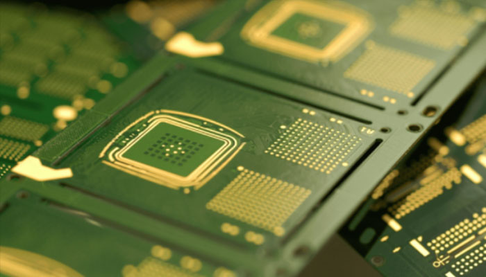
*High reliability
*High density layout
*Excellent Signal Integrality, SI
*Excellent Electromagnetic Compatibility,EMC
| Layer | 2-60 |
| The Width/Length | Width:600mm , Length 900mm |
| Line Width/Space | Inner : 3/3mil, Outer : 3/3mil |
| Minimum Drilling Diameter | 0.10mm(Mechanical Dilling), 0.075-0.1mm(Laser Driling) |
| Minimum Ring Width | 4mil |
| Board thickness | 0.2-10mm |
| Finished Copper | Inner : 8 OZ, Outer : 10 OZ |
| Spacing Between Hole And Conductor | Layer≤6: 5mil, 7≤Layer≤11: 6mil, Layer≥12: 8mil |
| Plate Thickness And Aperture Ratio | 1:1 (Blind Via); 16:1(Through Via) |
| Dimension Accuracy | +/-0.10mm(specially 士0.05mm) |
| Surface Processing Method | ENIG、ENEPIG、 HASL、FLASH GOLD、HARD GOLD、OSP |
· Experience in making various modules
· 24-hour delivery capability, effectively assisting customers in market development
· Mature and reliable blind burial process, in tray hole process, and half hole process
· Stable and reliable quality
· Special structure PCB production ability
· Process capability to adapt to special environmental requirements
· Obtaining long-term recognition from multiple medical clients
· Small size, fine PCB to meet the needs of portable products
· High reliability PCB product quality control
· Meet the technological research and development of new energy vehicles
· Strictly follow the IATF 16949 management system for operation


